Rajasthan Board RBSE Class 12 Physics Chapter 16 Electronics
RBSE Class 12 Physics Chapter 16 Text Book Exercise with Answers
RBSE Class 12 Physics Chapter 16 Multiple Choice Type Questions
Question 1.
At absolute zero temperature intrinsic germanium and intrinsic silicon; are :
(a) More conductor
(b) Good semiconductors
(c) Ideal insulator
(d) Conductors
Answer:
(c) Ideal insulator
Question 2.
In insulators the forbidden energy gap between valence band and conduction band is of ………. value :
(a) 1 eV
(b) 0.6 eV
(c) 0.1 eV
(d) 0.01 eV
Answer:
(b) 0.6 eV
Question 3.
At room temperature in intrinsic silicon the number of charge carriers per unit volume is 1.6 × 10¹⁶/m3. If mobility of electrons is 0.150 m2V-1 s-1 and mobility of holes is 0.05 m2V-1 s-1 then conductivity of silicon in (Ω-1m-1) is :
(a) 1.28 × 10⁻⁴
(b) 3.84 × 10⁻⁴
(c) 5.12 × 10⁻⁴
(d) 2.14 × 10⁻⁴
Answer:
(c) 5.12 × 10⁻⁴
Question 4.
If a NPN transistor is used as an amplifier then;
(a) Electrons move from base to collector
(b) Holes move from emitter to base
(c) Holes move from base to emitter
(d) Electrons move from emitter to base
Answer:
(d) Electrons move from emitter to base
Question 5.
The Boolean equation for given circuit will be :
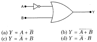
Answer:
(c)
Question 6.
For any ‘AND GATE’ the three inputs are A, B and C then the output Y will be;
(a )Y = A . B + C
(b) Y = A + B + C
(c ) Y = A + B . C
(d) Y = A . B . C
Answer:
(d) Y = A . B . C
Question 7.
The current amplification factor for common base circuit of a transistor is 0.95. When emitter current is 2mA then base current is :
(a) 0.1 mA
(b) 0.2 mA
(c) 0.19 mA
(d) 1.9 mA
Answer:
(a) 0.1 mA
Question 8.
The forbidden energy gap in germanium is 0.7 eV. The wavelength whose absorption is done by germanium is :
(a) 35000 Å
(b) 17700 Å
(c) 25000 Å
(d) 51600 Å
Answer:
(b) 17700 Å
Question 9.
The logic gate obtained by two NAND gate is :
(a) AND gate
(b) OR gate
(c) XOR gate
(d) NOR gate
Answer:
(a) AND gate
RBSE Class 12 Physics Chapter 16 Very Short Answer Type Questions
Question 1.
What is the direction of diffusion current in junction diode?
Answer:
It flows from P region to N region.
Question 2.
Write down the relation between a and p (current amplification factor) of the transistor.
Answer:
β = \(\frac{\alpha}{1-\alpha}\) or α = \(\frac{\beta}{\beta+1}\)
Question 3.
Can in any forward biased PN junction present potential difference can be measured by a voltmeter connected at the ends of the junction?
Answer:
No.
Question 4.
Make truth table for OR gate.
Answer:
Truth table for OR gate
| A | B | Y = A + B |
| 0 | 0 | 0 |
| 1 | 0 | 1 |
| 0 | 1 | 1 |
| 1 | 1 | 1 |
Question 5.
Write down the name of that logic gate in which the output is 1 when all the inputs are 1.
Answer:
AND Gate.
Question 6.
To use the transistor as an amplifier which junction is reverse biased?
Answer:
Base-collector junction.
Question 7.
What will be the value of a for that transistor for which β = 19?
Answer:
\(\alpha=\frac{\beta}{\beta+1}=\frac{19}{19+1}=\frac{19}{20}=0.95\)
Question 8.
The diode shown in the figure is in which biasing?
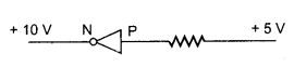
Answer:
The diode shown in the figure is reversed-biased (∵ VN > VP).
RBSE Class 12 Physics Chapter 16 Short Answer Type Questions
Question 1.
What is rectification? Draw the figure of bridge wave rectifier.
Answer:
Rectifier : The device employing diode, used to convert an alternating current into direct current, is known as rectifier.
Full wave rectifier : In this four junction diodes form the bridge circuit. It converts the whole cycle of applied A.C. signal into D.C. signal.
Question 2.
In a transistor why is the base made thin in comparison to the emitter and collector?
Answer:
The base of a transistor is kept very thin compared to the collector and emitter so that most of the carriers (carriers means electron in case of npn transistor and holes in case of pnp transistor) pass to the collector, injected from the emitter i.e, less number of electron-hole recombination take place and whole current emitted from emitter with a slight difference is passed to the collector.
Question 3.
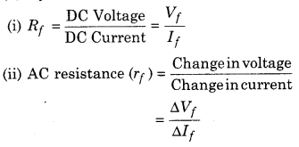
Make the full I-V characteristic curve for ideal PN junction diode. Define dynamic resistance in forward biased state.
Answer:
Dynamic resistance : A P-N junction diode allows electric current in one direction and blocks electric current in another direction. It allows electric current when it is forward biased and blocks electric current when it is reverse biased.
When forward biased voltage is applied to the P-N junction diode, the width of depletion region decreases. However the depletion region cannot be completely vanished. There exists a thin depletion region or depletion layer in the forward biased diode. Therefore, a thin depletion region and atoms in the diode offer some resistance to electric current. This resistance is called forward resistance.
In a forward biased p-n junction diode two types of resistances takes place based on the voltage applied.
(i) Static resistance or DC resistance
(ii) Dynamic resistance or AC resistance
Question 4.
What do you understand by logic gate? Draw the symbol for XOR gate and also the truth table.
Answer:
A logic gate is an elementary building block of a digital circuit. Most logic gates have two inputs and one output. A logic gate is a digital circuit that follows certain logical relationship between the input and output voltages. The five common logic gates used are OR gate, AND gate, NOT gate, NOR gate and NAND gate.
Each logic gate is indicated by a symbol and its function is defined by a truth table that shows all the possible input logic level combinations with their respective output logic levels. Truth tables help to understand the behaviour of logic gates. These logic gates can be realised using semiconductor devices.
The Boolean expression for XOR gate is :
Y = A ⊕ B
When any one of the input signals A or B has value 1 then only Y = 1. If the two inputs are 0 or 1 then output is 0. Hence, truth table for this gate is :
| A | B | Y = A ⊕ B |
| 0 | 0 | 0 |
| 0 | 1 | 1 |
| 1 | 0 | 1 |
| 1 | 1 | 0 |
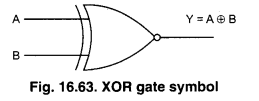
The XOR gate symbol is shown in the figure 16.63. The truth table for the expression;
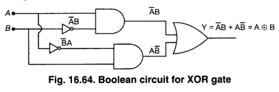
A ⊕ B = \(A \overline{B}+\overline{A} B\)
| A | B | \(\overline{A}\) | \(\overline{B}\) | \(A \overline{B}\) | \(\overline{A} B\) | \(A \overline{B}+\overline{A} B\) |
| 0 | 0 | 1 | 1 | 0 | 0 | 0 |
| 1 | 0 | 0 | 1 | 1 | 0 | 1 |
| 0 | 1 | 1 | 0 | 0 | 1 | 1 |
| 1 | 1 | 0 | 0 | 0 | 0 | 0 |
Hence, by using Boolean expression \(A \overline{B}+\overline{A} B\) (XOR) gate can be constructed. This is shown in the figure (16.64) in which we have used AND, OR and NOT gates.
Question 5.
Draw the transistor based circuit diagram for NOT gate and also give its truth table.
Answer:
NOT Gate
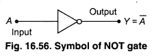
This is the most basic gate, with one input and one output. It produces T output if the input is ‘0’ and vice-versa. That is it produces an inverted version of the input at its output. This is why it is also known as an inverter.
The Boolean expression is given by; Y = \(\overline{A}\)
\(\overline{A}\) means NOT A meaning which is not A. (∴ A = 0, Y = \(\overline{0}\)= 1) and (A = 1, Y = \(\overline{1}\) = 0) . The truth table is given as follows
| A | Y – \(\overline{A}\) |
| 0 | 1 |
| 1 | 0 |
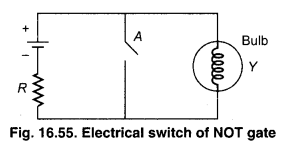
The sign for NOT gate is shown in the figure (16.55). It is also represented by an electrical circuit. When switch is on (1) then Y (bulb) is off (0). When switch is off (0) then Y is lighted (1). Figure (16.56) shows NOT gate sign.
For NOT gate transistor is used. A simple circuit is shown in the figure (16.57), in which an NPN transistor is used. The base B of the transistor is connected with the terminal A. Emitter E is earthed and collector C is connected to the positive end of direct current VCC = (5 V). Y is the potential difference of collector C relative to potential difference.
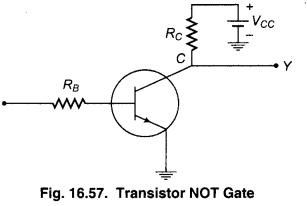
When, input terminal A is earthed then VA = 0 is also earthed. In this the base current is zero, when emitter current is zero the collector current is also zero, whereas the transistor is in cut off state.
Now if relative to earth + 5 V voltage is used (meaning A – 1) then base-emitter junction is forward biased. Now base current, emitter current and collector current all are present. If the values of RVB and RVC are chosen in such a way the collector current is high then transistor is in saturation state. In this state, the potential drop is + 5 V and Y = 0.
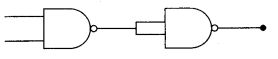
Question 6.
Write down the Boolean expression for given logic circuit. Draw truth table for it.
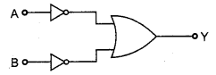
Answer:
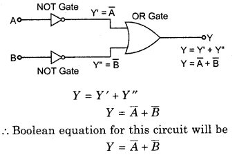
| Input | Outputs of NOT gates | Final output by OR gate Y = A + B (∵ Y=Y’+ Y”) | ||
| A | B | Y’ = A | Y” = B | |
| 0 | 0 | 1 | 1 | 1 |
| 0 | 1 | 1 | 0 | 1 |
| 1 | 0 | 0 | 1 | 1 |
| 1 | 1 | 0 | 0 | 0 |
Question 7.
Draw the circuit used for voltage regulation in a zener diode and also explain its process in short.
Answer:
Zener Diode
In reverse biasing arrangement of P-N junction diode we saw that in the state of breakdown voltage the reverse current of the diode is not less but increases rapidly; but the potential at the ends of the diode remains approximately equal to the breakdown voltage meaning remains constant.
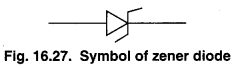
For any diode; breakdown voltage depends on the quantity of impurities mixed. Therefore, according to the quantity of the impure element any special breakdown voltage diode’s fabrication can be done. When any diode is so formed for any special breakdown voltage that in reverse biasing also at breakdown voltage it works without being damaged; then such type of diode is called zener diode. With the help of various quantities of impurity mixed today the diodes are available of less than 1 volt and in hundreds volt also. The sign of zener diode is shown in the figure (16.27).
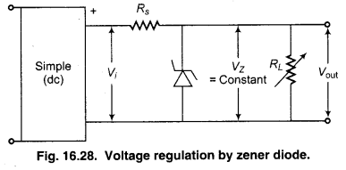
‘When the current flowing through the breakdown point from the zener diode is increased highly still the potential difference at both its ends is constant. This property makes its use for voltage stabilization and voltage regulation. We know that in an ordinary dc power supply with the use of rectifier and equalizer filter, ac is changed to dc. In such type of power supplies when there is change in load current, the value of dc voltage also changes. Therefore, in such situations where current is to be obtained at constant dc voltage such power supply cannot be used. With the help of a zener diode the output voltage of a power supply can be kept constant.
Figure (16.28) shows a power supply whose output voltage is assumed to be Vi and a resistance Rs and a zener diode are connected at its output terminals. A load resistor RL is parallel to the zener diode. The zener diode is so selected whose breakdown voltage Vz is equal to the constant value of that dc voltage which is to be obtained at load resistor RL. Zener diode is so placed in the circuit that it is in reverse biasing state. If the value of Vi is more than Vz then the diode comes in breakdown region and the potential Vz remains at its ends. Since RL is parallel to the diode, hence on it also there would be Vz potential. If the value of RL is changed then also it will have Vz potential. In this way the output voltage at both the ends of a zener diode is stable. The resistance Rs is so selected that the diode is not damaged by the thermal energy due to the increase in the zener current. This value of current is acknowledged by the data sheet given by the zener diode manufacturing company.
RBSE Class 12 Physics Chapter 16 Long Answer Type Questions
Question 1.
Differentiate between conductors, insulators and semiconductors on the basis of energy band principle. Explain the process of electrical conductance in intrinsic semiconductors.
Answer:
Classification of Conductor, Insulator and Semiconductor
Electrical conductivity is a physical quantity whose range is very wide. On one hand we know about metals whose electrical conductivity is very high on the other hand there is quartz, mica like insulators whose electrical conductivity is very low. Such substances are also known whose conductivity is very less than metals at normal temperatures but very high than insulators. These are called semiconductors.
The conductivity of semiconductors is not only between conductors and insulators but also the change in the conductivity with temperature is very interesting. Near absolute zero their behaviour is similar to insulators but as the temperature increases the conductivity also increases which is opposite to the projected behaviour of metals. The following questions are not answered by the principle related to electrical conductivity which you are will versed with :
- Why are the conductivities of solid substances different?
- Why does any substance show the behaviour of a semiconductor?
- Why is the change in conductivity with temperature different for metals and semi¬conductors?
On the basis of the principle of energy bands in solids and answering the questions, these are divided into conductors, insulators and semiconductors. Every solid substance has its own band construction which defines its electrical conductance behaviour.
Intrinsic Semiconductors
Those semiconductors in which there is no impurity are called intrinsic semiconductors. In ideal state in this type of intrinsic semiconductors there should be atoms of only that semiconductor. But in reality it is not possible to get such type of crystal. Therefore, if in a semiconductor material the number of impure atoms and the number of semiconductor atoms is in the ratio 1 : 108 or less than that then it is considered as an intrinsic semiconductor. To study the properties of semiconductors here we take the example of silicon and germanium.
Silicon and germanium both are the members of fourth group in the periodic table and their valency is 4. Their electronic configuration is as follows:
Ge (32) = 1s2 2s2 2p6 3s2 3p6 3d10 4s2 4p2
Si (14)= 1s2 2s2 2p6 3s2 3p2
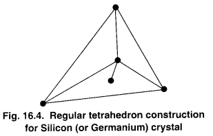
In the crystal construction of both these elements the atom is in an ordered array in such a way that each atom is inside a regular tetrahedron and on the four corners there are its other nearby atoms.
Figure (16.4) shows one such tetrahedron unit. Every valence electron of the atom makes a covalent bond with the valence electron of the nearby atom. In this way every atom is connected with the nearby atoms through covalent bonds. In every covalent bond there are two electrons. For convenience in study; figure (16.5) shows the two dimensionalform of crystal construction of germanium; which is also applicable for silicon.
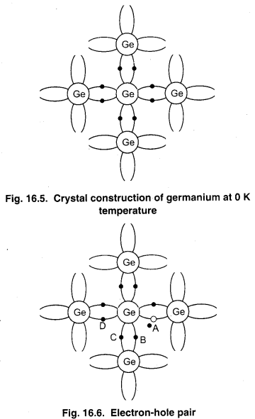
At absolute zero (0 K) also the valence electrons are bonded in covalent bonds hence there is no free electron available for electrical conductivity. Due to this at absolute zero temperature intrinsic semiconductors behave as insulators. When the temperature of the crystal is increased then some valence electron gain thermal energy and break their covalent bonds and become free. These free electrons move in the crystal freely and participate in electrical conductance when the crystal is applied external electronic energy.
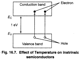
When one electron moves out of the covalent bond a vacancy is created. This vacancy is called a hole. The absence of electron is equal to the same magnitude positive charge. Hence, the hole can be assumed as a positive charge same in magnitude as that of an electron. As explained earlier, holes also participate in electrical conductance in semiconductors. In any semiconductor when a covalent bond breaks then a electrons hole pair is generated. At room temperature (300K) or a temperature close to it there are many electron hole pairs available at definite temperature. The production of electron hole pair is shown in figure (16.6).
At normal temperature electrons and holes do random motion in semiconductors. The random motion of hole can be understood in figure (16.6).
Suppose due to thermal energy an electron gets free from a covalent bond at position A, hence at this place a hole is generated. From a nearby atom, the valence electron breaks the covalent bond (at place B) and does transition to hole at position A. Then at A the covalent bond is complete; but now a hole is generated at position B. In this process very less energy is required which is very less than the necessary energy required for electron-hole pair production. The reason for this is that electron is doing transition from one bond to the other and all the electrons present in the bond are approximately of same energies. As shown in the figure due to the movement of electron form C to B the hole will do transition from B to C, etc. In this way in any semiconductor substance the electrons and holes both do random motion. Since, hole can be taken as the charge free electron +e, hence in a semiconductor both holes and electrons work as charge carriers and participate in electrical conductivity.
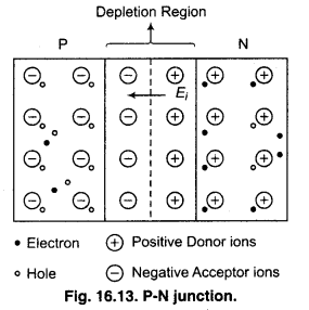
This process of hole electron pair production of intrinsic semiconductors can also be explained by band principle. The forbidden energy gap in semiconductors is of leV. At absolute zero temperature the valence band is completely filled and conduction band is fully empty. Hence, semiconductors behave as insulators. When the temperature of the crystal is increased electrons get necessary thermal energy and are capable of crossing the forbidden energy gap. Such type of electrons reach the conduction band from the valence band and holes are generated in the valence band in place of electrons (figure 16.7). Due to transition of one electron from valence band to conduction band a hole is generated and here also electron hole pair can be understood. The electrons present in conduction band are called free electrons and do random motion, similarly in valence band holes do random motion.
Generally, the breaking of the covalent bond or the electron reaching the conduction band from the valence band both are same. It can also be said that due to thermal energy the covalent bond breaks and the electron reaches the conduction band from the valence band. Therefore, for this process the necessary minimum energy would be equal to band interval energy Eg. Here this questions is logical that at room temperature, 300 K the average kinetic of the electron is kT = 1/40 = 0.025 eV, whereas the necessary energy for transition is leV. Then how does an electron reaches the conduction bond from the valence band? Here it is necessary to consider that kT is the value of average kinetic energy and not that all electrons are of this energy. Very less number of electrons would be there of leV energy which would do transition form valence band.
It is clear from above discussion that in any intrinsic semiconductor at definite temperatures the number of electrons and holes is same. If in an intrinsic semiconductor per unit volume the number of free electrons and holes is n and p respectively then
n = p = ni
np = \(n_{i}^{2}\) …………… (1)
where n, is the intrinsic charge carrier density.
When the temperature of an intrinsic semiconductor is increased then compared to prior temperature more covalent bonds break meaning more electrons reach the conduction band from valence band and the number of electron hole pair increases. This means that ni is dependent on temperature and increase with temperature. In this way two different semiconductors, for example, silicon and germanium, if they are at same temperatures then since the value of forbidden energy gap Eg for them is different, hence, the semiconductor for which the value Eg is less that will have more covalents bonds to break or more of the electrons will do transition from valence band to conduction band. Clearly at same temperature for two semiconductors for which the forbidden energy gap Eg is not same; the value of intrinsic charge carrier density will not be same but would be more for the semiconductor with less Eg value. In this way in an intrinsic semiconductor the value of intrinsic charge carrier density ni is dependent on :
(i) temperature (ii) nature of semiconductor material. In mathematical form this dependency is shown by following formula;
\(n_{i}=A T^{3 / 2} \exp -\left[\frac{E_{g}}{2 k T}\right]\) ………….. (2)
Where T is absolute temperature, k is Boltzmann constant and A is another constant.
At same temperature, comparing intrinsic silicon {Eg = 1.1 eV) and germanium (Eg = 0.7 eV) there are more number electron hole pairs in intrinsic germanium than in intrinsic silicon.
Question 2.
What is P-N junction ? Explain the process during its formation on the junction surface. If this junction is forward biased then explain the effect on depletion layer.
Answer:
P-N Junction
When a P-type semiconductor is connected to a N-type semiconductor in atomic level in such a way that their connecting surface maintains the crystal construction continuously; then this connection surface is called P-N junction and the device so formed is called PN junction diode. Generally, by special techniques in single crystal of silicon and germanium, the impurities are so mixed that its one part becomes P-type semiconductor and the second part becomes N-type semiconductor, and the boundary between these two regions is called P-N junction. A P-N junction cannot be formed by pressing a P-type semiconductor over a N-type semiconductor because in this condition the connecting surface on the crystal construction is not continuous.
As the P-N junction starts, due to the concentration gradient across P and N-sides, holes diffuse form P-side to N side (P → N) and electrons diffuse form N-side to P-side (N → P). This motion of charge gives rise to diffusion current across the junction. When an electron diffuses from N → P, it leaves behind an ionised donor on N-side. This ionised donor (positive) charge is immobile as it is bounded to the surrounding atoms. As the electrons continue to defuse form N → P, a level of positive charge (or positive space-charge-region) on n side of the junction is developed. Similarly when a hole diffuses form P→ N due to concentration gradient, it leaves being an ionised acceptor (negative charge) which is immobile. As the holes continue to diffuse,a layer of negative charge (or negative space-charge region) on the P-side of the junction is developed. This space-charge region of either side of the junction together is known as depletion region as the electrons and holes taking part in the initial movement across the junction depleted the region of its free charges. (Figure 16.13).
Forward Biasing
When an external voltage V is applied across a semiconductor diode such that P-side is connected to the positive terminal of the battery and N-side to the negative terminal (figure 16.14); then P side is at higher voltage than N-side. This is said as forward biasing. In this situation, an external electric field, E is established at the junction which is directed in the direction, of P to N. It is opposite to the internal electric field, Ei in the junction. Due to this the value of barrier potential at the junction reduces and now holes of P-region and electrons of N region move towards the junctions. As a result, more number of holes and electrons reach the depletion layer and its width decreases. Due to reduction of the value of potential barrier on either side of the junction, more and more charge carriers are distributed. Holes of P-side move towards the direction of E and electrons of N-side move opposite to the direction of E. In this situation, diffusion current is more than drainage current.
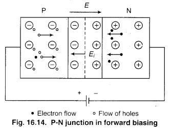
In the P-region near the positive end of the battery if an electons reaches this place by breaking the covalent bond then as a result of this process a hole is generated which moves towards the junction region. That electron moving through the connecting wires reaches the positive end of the battery. At the same time an electron starts its motion form the negative end of the battery and enters N-region and does motion towards the junction. In this way, there is flow of current in the junction. In P-region it is due to electrons; which are the majority-charge carriers for these regions. Therefore, this flow of current is due to the diffusion of majority charge carriers, clearly due to this biasing there is help in the flow of current in the junction, hence it is called forward biasing. In the external circuit the flow of current is only due to electrons.
If the voltage used by . the battery increased the potential barrier will reduce, more majority charge carriers will diffuse in the junction regions and the value of electric current will increase. Since, the flow of current is easily flowing through the junction, hence, the resistance of the junction will be very small in this case.
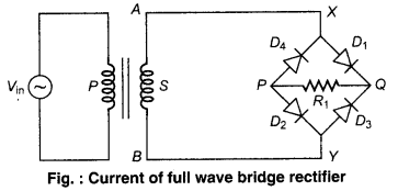
Question 3.
Draw the figure of full wave rectifier used to change AC to DC and explain its working.
Answer:
Full Wave Rectifier
In a full wave rectifier circuit the output voltage current is obtained for both the half cycles of input alternating voltage. Here two junction diodes are so used that one diode represents the positive half cycles of input ac and the other represents the negative half cycles. Figures (16.23) shows a circuit of full wave rectifier.
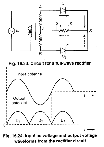
Here, the P-side of the diodes are connected to the ends of the secondary of the transformer. The N-side of the diodes are connected together and the output is taken between this common point of diodes and the midpoint of the secondary of the transformer. So for a full wave rectifier the secondary of the transformer is provided with a center tapping end so it is called center tap transformer. Suppose, the input voltage to A with respect to the centre tap at any instant is positive. It is clear, at that instant, voltage at B being out of phase will be negative. So diode D1 gets forward biased and conducts (while D2 being reverse biased is not conducting). Hence, during the positive half cycle we get an output current (and a output voltage across the load resistor RL). In the course of the ac cycle when the voltage at A becomes negative with respect to centre tap, the voltage at B would be positive. In this part of the cycle diode D1 would not conduct but diode D2 would giving an output current and output voltage (across R) during the negative half cycle of the input ac. Thus, we get output voltage during both the positive as well as negative half of the cycle. Obviously, this is a more efficient circuit for getting rectified voltage or current than the half wave rectifier.
For a full wave rectifier a centre tap transformer is necessary. Here normal transformer cannot be used. If the current is to be obtained at high voltage then this transformer should be step up transformer and if the current is to be obtained at low voltage then the transformer should be step down transformer.
Question 4.
Draw and explain the arrangement of characteristic curve for forward and reverse biasing of any P-N junction diode. Also make the figure of the curves.
Answer:
Forward Bias Characteristics
For the V-I characteristics of a forward biasing P-N junction diode the experimental circuit arrangement is shown in the figure (16.17).
Here the applied voltage V on the diode is changed by the potential divider arrangement which can be easily read by the voltmeter connected in parallel to the diode. The current I flowing in the diode related to various values of voltages are noted by a milliammeter. In this way, the curve obtained for different values of V and I is shown in the figure. (16.18), which is also called as the P-N junction diode forward bias characteristic curve.
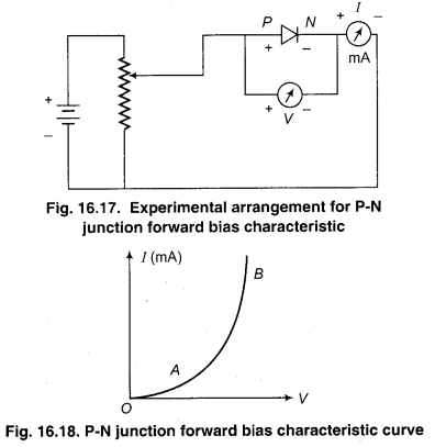
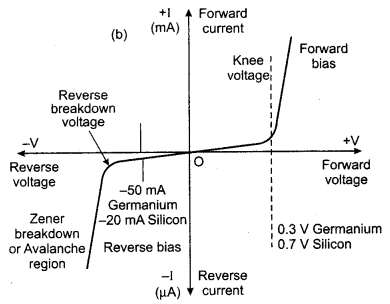
In forward biasing for every less value of voltage, (for Ge is 0.3 V and for Si is 0.7 V) the forward current is very less. The reason for this is that the value of applied voltage is less than the potential barrier due to which the flow of the current is not uniform. This behaviour of the diode is represented by the OA part of the curve. When the value of applied potential is more increased the current in the diode increases exponentially. This behaviour is shown by part AB. The potential at which the current’s value increase very rapidly is called the diode’s knee voltage or cut in voltage. For germanium diode its value is approximately 0.3 V and for silicon diode its value is 0.7V.
Reverse Bias Characteristics
For the V-I characteristics of a reverse biasing P-N junction diode the experimental circuit arrangement is shown in the figure 16.19. (a). Here with the help of a potential divider arrangement the P and N ends of the diode are connected to the negative and positive ends of the battery. Due to the reverse current being very small a miroammeter is used in place of milliammeter in this circuit. At different reverse potential the related different reverse current value are noted and a curve is drawn as shown in the figure 16.19(b).
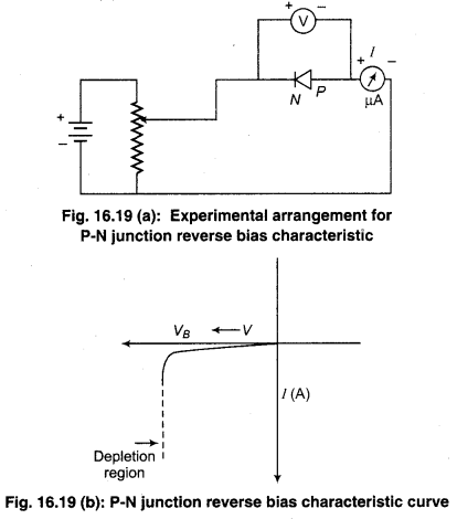
As explain in previous part in reverse biasing, the current is very small as it is due to minority- charge-carriers. and remains constant till the time the reverse potential reaches the value of breakdown voltage (VB). The reverse current increases very rapidly with a slight increase in the breakdown voltage.
For a semiconductor diode the complete figure for forward biasing and reverse biasing characteristic curve is shown in the figure 16.19.(c). If we consider the curve then in forward biasing more current (~ mA) flows and in reverse biasing (µ or nA) less current flows. As a result P-N junction diode is a unidirectional device. The characteristic curve of the diode also shows that this device do not follow Ohm’s law and hence is a non-linear device.
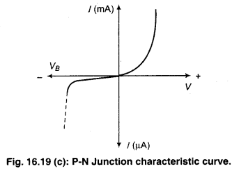
The dependency of current I flowing in the diode on the biasing V is given by following equation;
I = Is[\(\exp \frac{q V}{k T}\) – 1]
Where q = 1.6 × 10¹⁹ C, /e is Boltzmann constant, T is the temperature of the junction and V is the potential difference on the junction. Is is saturation current.
In forward biasing when V is positive then;
\(\exp \frac{q V}{k T}\) >> 1
then, I = Is\(\exp \frac{q V}{k T}\)
And current increases exponentially with the voltage. In reverse biasing when V is negative then;
\(\exp \frac{q V}{k T}\) << 1
∴ I ≈ Is
And in reverse biasing the current is almost constant.
The above equations are similar to the characteristics curve of germanium diode. The diode made of silicon follows this equation only in qualitative form and for both the types of diode in reverse biasing this equation is not true for potential higher than breakdown voltage
Question 5.
What is junction transistor? Make the necessary diagram and explain the working of a p-n-p transistor.
Answer:
Junction Transistor
A simple junction transistor generally is a unit crystal of an extrinsic semiconductor (silicon or germanium) in which three regions of different conductivity are present. The width of the middle region is less then the other two regions width and the nature of the semiconductor in this region is different than the other two regions. In this way we get two type of junction transistors which are called PNP and NPN respectively. In any PNP transistor, there are two P-types semiconductor regions and a N-types semiconductor is sandwiched between them with very less width. Similarly in an NPN transistor there are two N types semiconductor regions and a P-type semiconductor is sandwiched between these two with very less width.
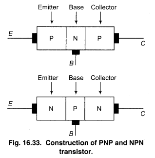
The middle region in both the types of transistors is called the base (B) and out of the outer parts one is called the emitter (E) and the other is called the collector (C).[Figure (16.33)]. In all the three regions there is a metallic electrode and a lead through which the transistor can be connected to external electric field. To whichever part the lead is connected according to that, the name is kept E lead, B lead or C lead.
The emitter and collector are of the same type of semiconductor (P or N) but the quantity of impurities mixed in them is different; also the collector region is bigger in size than the emitter. Due to this physical and electrical properties are different meaning, they individually have their special work. And hence they cannot be interchanged and used.
Emitter is basically doped because its work is to provide majority charge carrier in large numbers to the base. There is very less doping in base; also it is of very less width so that it does not provide opposite nature charge carrier in large number for recombination to the majority charge carriers coming from emitter. The work of the collector is to collect the majority charge carriers which pass through the base. Here the doping is less than the emitter but more than the base meaning it is medium.
The connecting region of collector-base is bigger then the connecting region of emitter-base. Due to this it does the collection of the charge carriers very well and the transistor when used in the form of an amplifier helps in rapid diffusion of the generated heat. In this way there are two P-N junctions in these transistors which are E-B junction (emitter-base junction) and B-C junction (base-collector junction). Principally, both these junction have a relationship between them. (Figure 16.34).
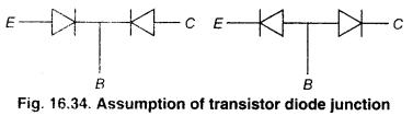
But here it is necessary to acknowledge that if two different P-N junction are joined according to the figure (18,31) then the transistor will never be received, because in transistor, both these junctions are in the same crystal, whereas two diodes when joint a single crystal is not possible. The width of the base of the transistors is in micrometer, hence both these junctions are very close.
Transistor when used in the form of an amplifier the emitter-base junction is always in forward biasing and base collector junction is always in reverse biasing. Due to this the majority charge carriers always flow from the emitter towards the base, but the current flowing in ths junction can be of the nature flowing from emitter to base (E to B) or base to emitter (B to E), These two different directions of the electric current are used to differentiate between the signs of PNP and NPN transistor. These symbols are shown in the figure (16.35).
The line part having an arrow sign represents the emitter part, the middle line part represents the base and third line part represents the collector. The arrow head shows the flow of current. Since in forward biasing state the emitter base junction of the PNP transistor the majority of holes from the P-type emitter move towards the N-type base hence, the current will flow in the junction from E to B. Therefore, in the symbol of PNP transistor the arrow head shows from E to B. Similarly, in NPN transistor in reverse biasing state the majority number of electrons move form N-type emitter to P-type base hence the current will be in the direction from B to E.
Operation of Transistor
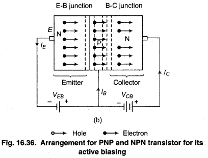
For any transistor to work efficiently E-B junction is placed in forward hosing and B-G junction is placed in reverse biasing. In this state the conduction of the art he biasing output for transistor is in active state. Figure 16.36 (a) and (b) shows NPN and PNP transistor, in both the figure the depletion region related to both the junctions are shown.
Since, E-B junction is forward biased and the doping in emitter is intense hence, E-B junction will be narrow. Whereas B-C junction is reverse biased hence it is broader. The applied forward biased potential difference VE value is small at E-B junction (0.5 – 1 V) and the applied reverse biased potential difference VCB value is more at B – C junction (5 to 15 V).
If we consider the circuits of PNP transistor shown in the figure 16.36 (a). Since, E-B junction is forward biased hence E region’s (P-type) majority charge carriers ‘holes’ will diffuse through this junction in large numbers. This is known as the injection of the holes from the emitter to the base. Similarly in the N-type semiconductor the electrons pass through the junction and reach emitter. The direction of both charge carriers is in opposite direction but the current related to them flows from E to B. This current is called emitting current IE which is both due to the holes and electrons. But due to less doping in base region for PNP transistor this current is basically due to holes.
The nature of the injected holes from the emitter to the base is of recombination with the electrons present in the base. But. due to the thin base and less dopped base very less hole (lees than 5%) recombine with the electrons, and majority of holes pass base collector junction and reach the collector. Since the collector terminal is negative hence these holes reach the collector terminal very easily and in this way generate collector current IC .
Some holes injected form the emitter to the base recombine with the electrons in the base and generate the base current IB of very less value. For every electron destroyed in the process of recombination the negative end joined with the base of battery VEB release one electron in the base. Therefore, here base current IB flows through the base terminal B. For a PNP transistor the Is current direction IE , IB and IC are shown in the figure 16.36 (a).
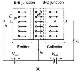
For the complete transistor shown in the figure if Kirchhoffs current law is used then, it is very clear that emitter current will be equal to the sum of base current and collector current, meaning;
IE = IB + IC …………… (14)
Here IB << IE and IB << IC Since, E-B junction is forward biased hence its forward resistance, is very less, and B-C junction is reverse biased hence its reverse resistance is maximum. Due to this it is observed that at emitter junction current IE will be more than the current collector junction. But from equation (14) IB is very less hence; IC ≈ IE. Hence from the view of operation transistor is a device which transfers the current IE from the circuit of very low resistance forward biased E-B junction) to the high resistance (reverse biased B-C junction keeping the same value IC (IC ≈ IE). For the transfer process of current this device is named by the combination of two words transfer resistor which is very well known as transistor.
In other words, it can also be said that in transistor the process of operation of current at B-E junction is very high on the collector current. Since the value of VEB is high hence both emitter current and collector current are more.
The above description can also be used for the active operation of NPN transistor. In this transistor majority charge carriers will be electron; which when injected form the emitter of N-type to the base of P-type reach the collector and produce collector current IC. Figure 16.36(b) shows the directions for IE, IB and IC for an NPN transistor.
The emitter current in a NPN transistor is mainly because of electrons. Whereas both transistors PNP and NPN are used but due to the mobility of electrons being higher than the holes, in high frequency circuits NPN transistors are more effective
Question 6.
Draw the circuit arrangement and also explain the characteristics curves for any common emitter configuration transistor. Also make the figures of curves and write the formula for voltage gain and current gain.
Answer:
Common Emitter Configuration
In this configuration emitter (E) input circuit and output circuit both are common. The potential difference between base and emitter is called potential difference input voltage whereas potential difference between collector and emitter is called output voltage. The basic arrangement for this configuration is shown in the figure 16.37 (b). Here base current IB is input current and collector current IC is output current.
For a PNP transistor when used to draw common emitter characteristic curve the circuit is shown in the figure (16.41). With the help of battery VBB and the potential breakdown arrangement R1 forward biasing VBE is provided to the base-emitter junction. The measure of VBE is done by the voltmeter present between base and emitter ends. Here, the value of base current IB is very low(~ A) hence it is measured by micro-ammeter. The potential difference VCE between the collector and emitter due to the battery VCC and potential breakdown arrangement R2 is measured by the voltmeter and collector current IC is measured by milliammeter.
Here, this question is necessary that how does the base-collector junction is provided forward biasing, since there is no battery between them? To answer this question see figure (16.41) carefully.
Here, both base and collector are connected to the negative ends of the circuits of their batteries (VBB and VCC ). If the magnitude of VCE is higher than VBE then base (A-type) will be at negative potential than collector (P-type).
In other words, A-type base is at a higher positive potential than P-type collector, clearly this junction will be reverse biased.
Input Characteristics : Here output voltage VCE is kept constant and the changes in input current IB are studied related to the input voltage VBE. For this with the help of R2. VCE is kept at a constant value. Now with the help of R1 the value of VBE is increased from zero and changed to discrete values and the value of IB related to increased. A graph is drawn between IB and VBE. The same process is repeated for other values of VCE . The graph of curves so obtained are called the input characteristics of common emitter configuration. Figure (16.42) shows the characteristic curves for three constant values.
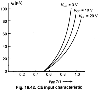
Dynamic Input Resistance
The dynamic input resistance for common emitter configuration of transistor is given by following formula :
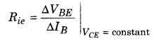
The value of this approximately of 100 Ω. If this value is compared with common base circuit input resistance Rib then, Rie > Rib.
Output Characteristic : Here, input current IB is kept constant and the changes in output current IC related to output voltage VCE is studied. To calculate this with the help of R2 the value of VCE is changed and hence the value of IC increases. A graph is drawn between VCE and IC . This process is repeated for other values of IB. Hence, the group of curves so obtained are called output characteristics. These are shown in the figure (16.43).
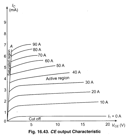
At any constant value of IB , VCE when increased from zero, IC very fast gets saturated. After this the value of IQ increases slowly. The line OA in figure (16.43) is called saturated line and the area between IC and this line is called saturated region. When IB = 0 then also IC is not zero, meaning when input current is zero still some output current flows.
The region between IB = o and VCE axis is called cut off region.
The remaining region apart from the cut off region and saturated region is called the active region. Here, the emitter-base junction is transistor is forward biased and the base-collector junction is reverse biased.
In active region IC is not dependent on VCE .
The dynamic output resistance Roe for this configuration is defined as follows :
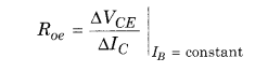
Since, IC does not change much with VCE (leaving the initial values of VCE ). Therefore, Roe is of 50-100 kΩ.
Current Amplification Factor
This is defined as the ratio of the change in collector current to the change in base current at a constant collector emitter voltage (VCE) when the transistor is in active state.
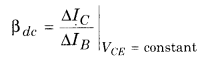
This is also known as small signal current gain and its value is very large.
β = \(\frac{I_{C}}{I_{B}}\)
Since, IC >> IB and ΔIC >> ΔIB. Therefore, (β dc and β both are grater than 1 meaning β >> 1.
Question 7.
What do you understand by amplification? Make the diagram of a p-n-p transistor common amplifier and explain the process of amplification and calculate the formula for voltage gain.
Answer:
Transistor Amplifier
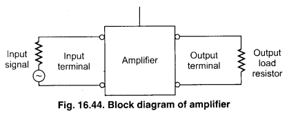
Amplifier is an active electronic device of which the amplitude of output signal obtained is more than the amplitude of the input signal applied on it. Input signal is generally alternating current or voltage (a.c.). the process of increase in the amplitude of the signal is called amplification. In this there is no change in the shape and frequency of the signal. The necessary energy required for the increase in the amplitude of the signal is obtained from the dc power supply in the amplifier circuit. Figure (16.44) shows the block diagram of an amplifier.
One type of amplifier, which is used in our daily life and which is known to us is the sound frequency amplifier. With the help of a microphone, the sound signals are converted into electrical signals of same frequency and hence injected in the amplifier and output of which high amplitude electrical signals are obtained which are again changed into sound signals by the loudspeaker. Hence, we hear a high intensity sound.
The ratio between output and input signals for an amplifier is known as amplification factor or gain. If the input signal voltage is Vi and output signal voltage is V0 then;
Voltage amplification factor or voltage gain
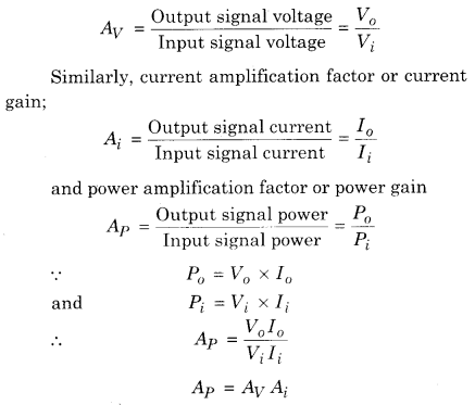
Hence, for amplifier all the three amplification factors are corelated.
Transistor, when used in the form of an amplifier its one terminal of input and output circuits, is common. Input signal whose amplification is to be done is used in the input circuit and output circuit has load resistor RL. The amplification process by a transistor is possible for both the configuration of common base and common emitter. But the voltage current and power gain for common emitter amplifier are more than the common-base amplifier.
Hence, here we will only study about common-emitter amplifier.
Common-Emitter Amplifier
Figure 16.45 shows a PNP transistor common-emitter circuit. Here, emitter is common for both the input and output circuits. With the help of battery VBB the emitter-base junction is provided forward biasing. Whereas with the help of battery VCC (> VBB ) reverse biasing is provided to the collector – emitter junction. V; is signal voltage whose amplification is to be done.
A load resistor RL is connected to output circuit on which amplified voltage V0 is obtained.
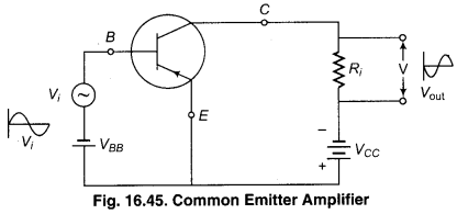
If alternative signal Vi is absent then potential difference VBE present on base-emitter junction is constant. Due to this the input current IB and the output current IC related to it is of constant and direct nature. In the presence of Vi the potential difference of base-emitter junction changes. If there is very less change in IB and change is IB and there is change in related collected current IC and change is iC. According to definition;
Current Gain :
Since, β >> 1, therefore output signal current is more than input current. Hence, in common emitter configuration the current is amplified. [In sign Aie the element e represents common emitter configuration.]
Voltage Amplification
Voltage amplification or voltage gain by definition;
Here, V0 – Alternating voltage generated on load resistor RL
= iCRL
and Vi = ibRie
where Rie is the input resistance in common – emitter configuration
\(A_{v e}=\frac{i_{c} R_{L}}{i_{b} R_{i e}}=\beta \times \frac{R_{L}}{R_{i e}}\)
\(\frac{R_{L}}{R_{i e}}\) is called the resistance gain for common-emitter configuration.
Therefore, Ave = Aie × resistance gain.
Because β >> 1, therefore RL and Rie are same hence;
If Ave ≈ β >> 1 then voltage amplification is possible. If RL > Rie, then Ave > β >> 1) more voltage resistance is obtained.
Question 8.
Write down the names of some diodes used for special purposes and make their circuit figures. Write about their working and uses in short.
Answer:
Special Purpose Diodes
Apart from rectification, P-N Junction diodes have other uses also. The diodes used for some special purposes are different form the diodes used for some other special purpose in properties, used semiconductor, quantity of impurities and construction, etc. Now we will study about some special purpose diodes.
Zener Diode
In reverse biasing arrangement of P-N junction diode we saw that in the state of breakdown voltage the reverse current of the diode is not less but increases rapidly; but the potential at the ends of the diode remains approximately equal to the breakdown voltage meaning remains constant.
For any diode; breakdown voltage depends on the quantity of impurities mixed. Therefore, according to the quantity of the impure element any special breakdown voltage diode’s fabrication can be done. When any diode is so formed for any special breakdown voltage that in reverse biasing also at breakdown voltage it works without being damaged; then such type of diode is called zener diode. With the help of various quantities of impurity mixed today the diodes are available of less than 1 volt and in hundreds volt also. The sign of zener diode is shown in the figure (16.27).
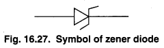
Photo Diode
The light of desired frequency when is falling on any semiconductor (electromagnetic radiation), then due to the energy obtained by the absorption, the electrons of the valence band of the semiconductor do make transition to the conduction band. In the such types of electrons a hole is generated corresponding to each electron in the valence band and hence in this way electron hole pair is generated. These electron hole pairs are different to those electron hole pairs generated by thermal energy. Clearly, in this process the conductivity of the semiconductor increases. Due to the incident light the increase in the conductivity of the semiconductor so observed is called photoconductivity and their effect is called photo-conductive effect. If the frequency of the photons of the incident light is v, and its energy hv is equal or more than the forbidden energy gap of the semiconductor Eg (hv ≥ Eg) then these photons shown above effect.
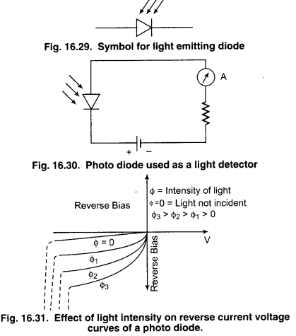
Photo diode is used in following devices:
- Light detection.
- Light operated switch.
- Reproduction of sound in films.
- For reading computer types and computer cards.
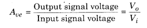
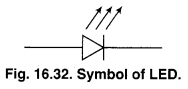
Light Emitting Diode (LED)
Light emitting diodes are those P-N junction diodes which in forward biasing emit light. When an electron present in the conduction band of semiconductor do transition make the hole present in the valence band recombination meaning, there is recombination of electron hole and then, in this process energy is released. Generally the electrons are at the minimum energy level of the conduction band (EC) and the holes are at the maximum energy level of the valence band (EV). Hence, energy released in the process is EC – EV = Eg meaning equal to the forbidden energy gap. In many semiconductor like silicon and germanium, this energy is released in the form of heat (thermal) but in gallium arsenide, phosphide (GaAsP) and gallium phosphide (GaP) like semiconductors, this energy is released in the form of visible light energy.
The intensity of light should be more for this. It is necessary that this type of recombinations are large in number. But for intrinsic and extrinsic both types of semiconductors such types of recombinations are in limited number. This is due to the reason that in intrinsic semiconductors the number of electrons hole pairs is less and in extrinsic semiconductors one type of charge carrier are in majority and the other type of charge carriers are in minority.
In semiconductors like GaP if the P and N region of the junction area the impurity is mixed in large quantity then the depletion region will be very thin. If the junction is in forward biasing then the large number of holes of P region move towards N region and the large number of electrons of N region move towards P region. Hence, near the depletion layer there would be large recombination of electrons and holes. As a result the emitted light will be of high intensity. The figure (16.32) shows a light emitting diode.
The semiconductor for LED is chosen as per the desired colour light. At present the LED lights of red, green, yellow, orange and blue colour are available. The LED is used for following purposes:
- In the form of indicator light.
- In the form of seven segment display unit.
- LED generating high intensity light are used in optical fibre communication.
- High intensity light giving LED bulbs.
Question 9.
Draw circuit diagram for two input diode OR gate and AND gate. Also explain their working and give truth table.
Answer:
OR Gate
An OR gate has two or more inputs with one output. The output Y is 1 when either input A or input B or both are 1s, that is; if any of the input is high, the output is high.
Since logic gates are based on such values for which only two values are possible 0 and 1, this type of Algebra is different. This type of Algebra is known as Boolean Algebra and the equations representing these relationships are called Boolean expressions.
For a two input OR gate if inputs are given as A and B respectively and output is F then Boolean expression is
Y = A + B
Here the + sign between A and B represents OR operation. Y = A + B means Y, A or B.
Where A = 0, 1 and B = 0, 1.
The truth table for this;
| A | B | Y = A +B |
| 0 | 0 | 0 |
| 1 | 0 | 1 |
| 0 | 1 | 1 |
| 1 | 1 | 1 |
It is clear from above table that out of the input values A and B if one or both are 1 then output Fis 1. When both A and B are zero then output F is also zero.
OR gate can also be explained by electrical switches connected in parallel. As shown in figure (16.49) the switches A and B are connected parallel and are connected with a battery and a bulb Y.
If A and B’s closed state (ON state) is represented by 1 and open state (off state) is represented by 0 and the lighted and unlighted situation of the bulb is also 1 or 0 then for this circuit there are four possibilities.
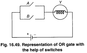
(i) If A and B both are open then there is no current in Y, hence bulb is not lighted. In mathematical form A = 0, B = 0 then Y = A + B = 0.
(ii) If switch A is closed (A = 1) and B is open (B = 0) then battery will flow the current through switch A and light the bulb Y, hence Y = 1.
∴ A = 1, B = 0 then Y = A + B =1.
(iii) If A is open and B is closed then also bulb will be lighted.∴A = 0, B = 1, Y = A + B = 1.
(iv) If A and B both are closed (A = B = 1) then bulb will be lighted (Y = 1). ∴ A = B = 1, Y = A + B = 1.
All the above four possibilities are according to the truth table. Figure (16.50) shows the symbol for OR gate.
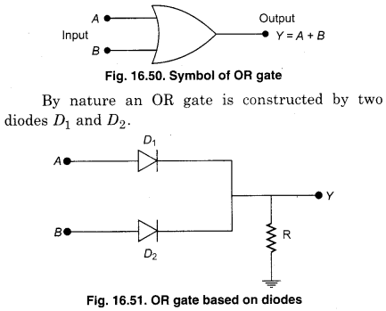
(i) The value of 0 V or 5 V is provided to the inputs A and B. 0 V is represented by 0 and 5V represented by 1. R is the resistance at output Y and the other end of resistance R is earthed.
(ii) When A = B = 0 meaning there is no signal then no diode will be operated and no potential drop at R or Y = 0. This is equal to the first row of the truth table.
If input A is 5 V (1) or B = 0 V (0) then diode Di will be forward biased and behave as closed switch hence is in operated state. If D1 is an ideal diode then there is no potential drop.
So, 5 V potential drop will be on resistance R with earth or will get Y = 1 position. This will be similar to second row of truth table.
(iii) If A = 0 and B = 5 V (1) then in place of D1, D2 will be in state of operation. Still Y = 1. This is similar to third row.
(iv) If A and B both the diodes are (5 V) then both diodes will be in operation. This will be similar to fourth row of truth table.
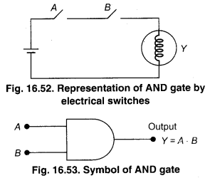
AND Gate
An AND gate has two or more inputs and one output. The output Y of AND gate is 1 only when input A and input B are both 1. The Boolean expression for this gate is represented as; Y = A . B
This represents AND operation. The above Boolean equation means, Y = A and B. The truth table for this:
| A | B | Y = A.B |
| 0 | 0 | 0 |
| 1 | 0 | 0 |
| 0 | 1 | 0 |
| 1 | 1 | 1 |
Hence, in AND gate when input of both is 1 then only output is 1.
The AND gate can be explained by electrical switches; (Figure 16.52). When both switches A and B are open (A = B = 0) then there is no current in circuit.
Hence, bulb Y is not lighted. This is equal to the first line of the truth table. If any of the two switches is open then also Y = 0. When both switches are closed (A = B = 1), then Y = 1, bulb is lighted. Figure (16.53) shows AND sign.
In behaviour AND gate is also obtained by the help of diodes. Figure (16.54) shows AND gate represented by diodes.
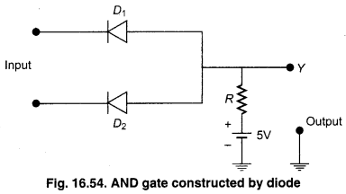
Here resistance R is connected with a battery of potential difference 5 V with the positive terminal and the negative end is earthed. Input terminals A and B are given 0 or 5 V level.
If A and B both are at zero potential (A = B = 0) then diodes D1 and D2 both are forward biased. This represents the first line of truth table.
If A and B any of the two has value 5 V and the other has 0 V, then diode A is in operation mode and B is in non-operation mode. If diode A is ideal then there will be no potential drop. This represents the third line. If A = B = 5 V then Y – 1 (5 V) hence this represents the fourth line of truth table.
RBSE Class 12 Physics Chapter 16 Numerical Questions
Question 1.
Calculate the electric current generated in an intrinsic germanium plate at room temperature whose area is 2 × 10⁻⁴ m2 and width is 1.2 × 10⁻³ m and a potential difference of 5V is applied. Intrinsic charge carrier density is 1.6 × 10⁶ /m3 for germanium at room temperature. The mobility of electrons and holes is 0.4 m2 V-1 s-1 and 0.2 m2 v-1 s-1.
Solution:
Given, Area of plate (A) = 2 × 10⁻⁴ m2
Width (l) = 1.2 × 10⁻³ m
Potential difference V = 5 V
Intrinsic charge carrier density n1 = 1.6 × 10⁶/m3
Mobility of electrons (µ2) – 0.4 m2V-1s-1
Mobility of holes (µn ) = 0.2 m2V-1s-1
So, current in Ge plate I = \(\frac{V}{R}\)
Question 2.
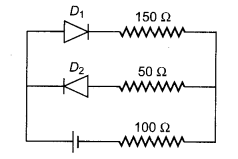
As shown in the circuit below the forward resistance of both diodes is 50 Ω and reverse resistance is infinite. If electric charge force is 6 V of the battery then calculate the current flowing through 100 Ω.
Solution:
It is given that forward resistance of both diodes D1 and D2 is = 50Ω. It is clear from given circuit diagram that diode D2 is in reverse-bias so it will not conduct. Only diode D1 will conduct as it is in forward-bias.
∴ Total resistance of circuit (R) = 50 + 150 + 100
or R = 300 Ω
So the current flowing through 100 Ω
I = \(\frac{V}{R}=\frac{6}{300}\) = 0.02 A
Question 3.
The current amplification is 0.99 for any transistor in common-base configuration. Calculate the change in collector current when there is 5.0 milliampere change in emitter current. What will be the change in base current?
Solution:
Current amplification α = 0.99
Change in emitter current ΔI = 5 mA
∵ α = \(\frac{\Delta I_{C}}{\Delta I_{E}}\)
∴ ΔIC = α • ΔIE = 0.99 × 5 = 4.95 mA
∵ ΔIE = ΔIE + ΔIC
=> ΔIB – ΔIE – ΔIC
= 5 mA – 4.95 mA
= 0.05 mA
∴ ΔIB = 5 × 10⁻⁵ A= 50 × 10-6 A = 50μA
Question 4.
For a PN junction the average value of a potential well is 0.1 V and the electric field 105 V/m is present at junction region. What will be the width of depletion layer for this junction?
Solution:
Average value of potential well VB = 0.1 V
Electric field at junction region E = 105 V/m
∴ Width of depletion layer for this junction
d = \(\frac{V_{B}}{E}\) {∵ E = \(\frac{V}{d}\)}
or d = \(\frac{0.1}{10^{5}}\) = 10-6 m
Question 5.
A transistor is connected in common emitter configuration. A power supply of 8V is there in the collector circuit and the potential drop of 0.5V is on the resistance of 800 12 connected in series with the collector. If current amplification factor is α = 0.96. Then calculate base current.
Solution:
Given VCC = 8 V, RL = 800 Ω and Vout = 0.5 V
Current amplification factor α = 0.96
We got output voltage in collector-circuit
Question 6.
In a common emitter amplifier an increase of 50 A in base current causes a 1.0 mA increase in collector current. Calculate current gain β. What will be the change in emitter current ? Calculate α with the help of β.
Solution:
Change in base current ΔIE = 50 µA
Change in collector current ΔIC = 1.0 mA
\(\therefore \beta=\frac{\Delta I_{C}}{\Delta I_{B}}=\frac{1.0 \mathrm{mA}}{50 \mu \mathrm{A}}=\frac{1 \times 10^{-3}}{50 \times 10^{-6}}=\frac{1000}{50}=20\)
So, the change in emitter current
ΔIE = ΔIB + ΔIC
= 50 µA + 1.0 mA
= 50 µA + 1000 µA = 1050 µA = 1.050 mA
Now, α = \(\frac{\beta}{1+\beta}=\frac{20}{20+1}=\frac{20}{21}\) = 0.9523
α = 0.95
Question 7.
Calculate the potential difference and the current between ends of zener diode in the given circuit. If load resistor RL = 2 kΩ ends has a potential difference of 15 V. The lowest working current of zener diode is 10 mA.
Solution:
Load resistance
RL = 2 kΩ = 2 × 10³ Ω
Potential difference at the end points of load resistance
V = 15V
∴ Current in RL
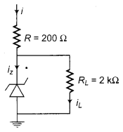
IL = \(\frac{V}{R_{L}}=\frac{15}{2 \times 10^{3}}\) = 7.5 × 10⁻³ Amp.
∴ IL = 7.5 mA
The lowest working current of zener diode
(Iz) = 10 mA
Current in circuit
I = IL + IZ
= 7.5 mA + 10 mA = 17.5 mA
Zener diode and load resistance (RL) are connected in parallel so potential difference between the current ends of zener diode = Potential at the ends points of RL = 15 V